


Automatic defect detection equipment for ship type vehicles
Automatic ejector pin module detection
Final appearance inspection of the chip
Chip heat dissipation cover flux detection
Automatic detection of adhesive for heat dissipation cover
Inverted chip filling adhesive detection
Chip inversion position detection
Automatic six-sided chip inspection
Fully Automated Wafer Optical Inspection Equipment
Automatic Wafer Sorter
OPE equipment
Cleaning machine loading and unloading modification equipment
E-rack equipment
E84 equipment renovation
Intelligent storage system
Tray packaging machine
Wafer packaging machine
Automatic wafer sorting machine
Autonomous Mobile Robot AMR
High altitude wafer conveyor line
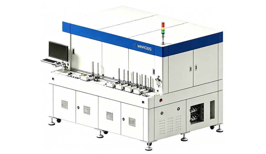
Equipment size: L * W * H 2300 * 2000 * 2200mm
Equipment function: High performance, fully automated optical inspection of semiconductor packaged integrated circuits (ICs), utilizing high-sensitivity detection of various component types and sizes through 2D and 3D measurements to determine the final packaging quality
Performance indicators:
Efficiency: 250pcs/H (QFN 120 * 120mm), 350pcs/H (BGA 75mm * 75mm)
Accuracy: The upper and lower surfaces can detect defects with a minimum thickness of 30um, and the four sides can detect defects with a minimum thickness of 30um. The 3D measurement has a repeatability accuracy of 10um;
• Misjudgment/overkill:<2% Underkill: 0%
Technical Features:
Five track design, three unloading tracks, capable of supporting up to 5 bin levels.
Four independent detection stations and component sorting stations operating in parallel have improved detection efficiency.
High sensitivity 2D and 3D measurement capabilities ensure the accuracy of detection.
• Unique high-precision side detection system that supports detection of BGA substrate bonding gaps, exposed copper, etc
Application scenario: Detection and quality control of packaged ICs
Applicable processes: FCBGA/WBBGA/QFN/LGA, etc

No. 88 Yangdong Road, Suzhou Industrial Park

+86-185-0151-0586

WeChat Official Account
COPYRIGHT (©) 2020 SUZHOU WINROBS TECHNOLOGY CO., LTD Su ICP Bei 19010085-2

