


Automatic defect detection equipment for ship type vehicles
Automatic ejector pin module detection
Final appearance inspection of the chip
Chip heat dissipation cover flux detection
Automatic detection of adhesive for heat dissipation cover
Inverted chip filling adhesive detection
Chip inversion position detection
Automatic six-sided chip inspection
Fully Automated Wafer Optical Inspection Equipment
Automatic Wafer Sorter
OPE equipment
Cleaning machine loading and unloading modification equipment
E-rack equipment
E84 equipment renovation
Intelligent storage system
Tray packaging machine
Wafer packaging machine
Automatic wafer sorting machine
Autonomous Mobile Robot AMR
High altitude wafer conveyor line
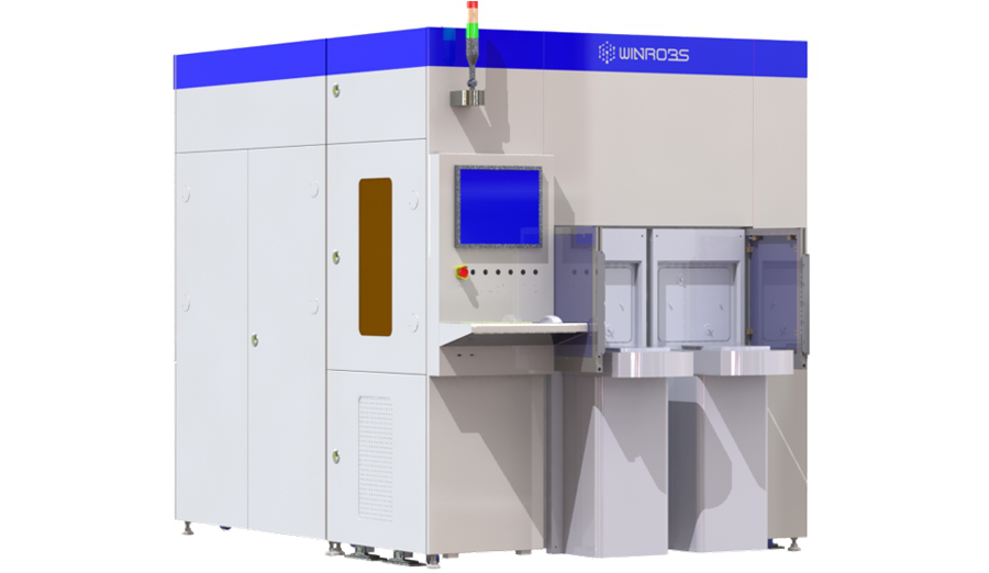
Equipment Name: Fully Automatic Wafer Optical Inspection Equipment
Equipment dimensions: L*W*H 2760*1850*2100mm
Device functions:
• Incoming wafer defect inspection
•RDL process inspection
•Bumping process inspection
• 2D+3D Bump finished product shipment inspection
• Supports SECS/GEM interface protocol
Performance indicators:
• Efficiency: 2D 30WPH@5X for 12 inch Wafer
• 3D 10WPH for full inspection of 12-inch wafer bumps
• Accuracy: minimum detectable defect size of 2*2 pixel, 3D repeatability accuracy of 0.3um
Technical Features:
• Self-developed high-precision 3D algorithm, capable of detecting Bumps with a diameter of 20um and a height of 20um
• Self-developed defect detection algorithm, combined with AI for inspection, achieving an accuracy rate of over 99%
• Vibration suppression technology ensures that the fluctuation error is less than ±1 pixel during high-speed flying scan
• Supports large warped wafer adsorption and AI ADC functionality
Application process: Bumping, RDL process
Applicable products: 6-inch & 8-inch, 8-inch & 12-inch bare wafers

No. 88 Yangdong Road, Suzhou Industrial Park

+86-185-0151-0586

WeChat Official Account
COPYRIGHT (©) 2020 SUZHOU WINROBS TECHNOLOGY CO., LTD Su ICP Bei 19010085-2

